A radio-electronic element made of semiconductor material, using an input signal, creates, amplifies, changes pulses in integrated circuits and systems for storing, processing and transmitting information. A transistor is a resistance whose functions are regulated by the voltage between emitter and base or source and gate, depending on the type of module.
Content
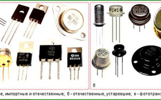
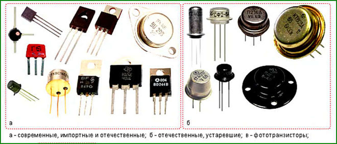
Types of transistors
Converters are widely used in the production of digital and analog microcircuits for zeroing static consumer current and obtaining improved linearity. The types of transistors differ in that some are controlled by a voltage change, the latter are regulated by a current deviation.
The field modules operate with increased DC resistance, high frequency transformation does not increase energy costs.If we say what a transistor is in simple words, then this is a module with a high gain margin. This characteristic is greater in field species than in bipolar types. The former do not have charge carrier resorption, which speeds up operation.
Field semiconductors are used more often because of their advantages over bipolar types:
- powerful resistance at the input at direct current and high frequency, this reduces the energy loss for control;
- lack of accumulation of minor electrons, which accelerates the operation of the transistor;
- transport of moving particles;
- stability with temperature deviations;
- small noise due to lack of injection;
- low power consumption during operation.
The types of transistors and their properties determine the purpose. Heating the bipolar type converter increases the current along the path from the collector to the emitter. They have a negative resistance coefficient, and mobile carriers flow to the collecting device from the emitter. The thin base is separated by p-n junctions, and the current arises only when moving particles accumulate and are injected into the base. Some charge carriers are captured by an adjacent p-n junction and accelerated, this is how the parameters of transistors are calculated.
FETs have another kind of advantage that needs to be mentioned for dummies. They are connected in parallel without equalizing the resistance. Resistors are not used for this purpose, since the indicator increases automatically when the load changes. To obtain a high value of the switching current, a complex of modules is recruited, which is used in inverters or other devices.
It is impossible to connect a bipolar transistor in parallel, the determination of functional parameters leads to the fact that a thermal breakdown of an irreversible nature is detected. These properties are related to the technical qualities of simple p-n channels. The modules are connected in parallel using resistors to equalize the current in the emitter circuits. Depending on the functional features and individual specifics, bipolar and field types are distinguished in the classification of transistors.
Bipolar transistors
Bipolar designs are produced in the form of semiconductor devices with three conductors. Layers with hole p-conductivity or impurity n-conductivity are provided in each of the electrodes. The choice of a complete set of layers determines the release of p-n-p or n-p-n types of devices. At the moment the device is turned on, different types of charges are simultaneously transferred by holes and electrons, 2 types of particles are involved.
Carriers move due to the diffusion mechanism. Atoms and molecules of a substance penetrate into the intermolecular lattice of a neighboring material, after which their concentration levels off throughout the volume. Transport occurs from areas of high compaction to areas of low content.
Electrons also propagate under the action of a force field around particles with an uneven inclusion of alloying additives in the base mass. To speed up the action of the device, the electrode connected to the middle layer is made thin. The outermost conductors are called emitter and collector. The reverse voltage characteristic of the transition is unimportant.
FETs
The field-effect transistor controls the resistance using an electric transverse field arising from the applied voltage. The place from which the electrons move into the channel is called the source, and the drain looks like the end point of entry of charges. The control voltage passes through a conductor called the gate. Devices are divided into 2 types:
- with control p-n-junction;
- MIS transistors with an insulated gate.
Devices of the first type contain a semiconductor wafer in the design, which is connected to the controlled circuit using electrodes on opposite sides (drain and source). A place with a different type of conductivity occurs after the plate is connected to the gate. A constant bias source inserted into the input circuit produces a blocking voltage at the junction.
The source of the amplified pulse is also located in the input circuit. After changing the voltage at the input, the corresponding indicator at the p-n junction is transformed. The layer thickness and the cross-sectional area of the channel junction in the crystal, which transmits the flow of charged electrons, is modified. The channel width depends on the space between the depletion region (below the gate) and the substrate. The control current at the start and end points is controlled by changing the width of the depletion region.
The MIS transistor is characterized by the fact that its gate is separated by insulation from the channel layer. In a semiconductor crystal, called a substrate, doped sites with the opposite sign are created. Conductors are installed on them - a drain and a source, between which a dielectric is located at a distance of less than a micron. On the insulator there is a metal electrode - a shutter.Due to the resulting structure containing a metal, a dielectric layer and a semiconductor, the transistors are given the abbreviation MIS.
Device and principle of operation for beginners
Technologies operate not only with a charge of electricity, but also with a magnetic field, light quanta and photons. The principle of operation of the transistor lies in the states between which the device switches. Opposite small and large signal, open and closed state - this is the double work of devices.
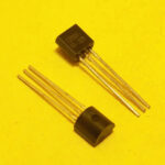
Together with the semiconductor material in the composition, used in the form of a single crystal, doped in some places, the transistor has in its design:
- conclusions from metal;
- dielectric insulators;
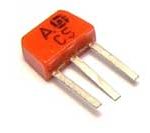
- case of transistors made of glass, metal, plastic, cermet.
Before the invention of bipolar or polar devices, electronic vacuum tubes were used as active elements. The circuits developed for them, after modification, are used in the production of semiconductor devices. They could be connected as a transistor and used, since many of the functional characteristics of the lamps are suitable for describing the operation of field species.
Advantages and disadvantages of replacing lamps with transistors
The invention of transistors is a stimulating factor for the introduction of innovative technologies in electronics. The network uses modern semiconductor elements, in comparison with the old lamp circuits, such developments have advantages:
- small dimensions and low weight, which is important for miniature electronics;
- the ability to apply automated processes in the production of devices and group stages, which reduces the cost;
- the use of small-sized current sources due to the need for low voltage;
- instantaneous switching on, heating of the cathode is not required;
- increased energy efficiency due to reduced power dissipation;
- strength and reliability;
- well-coordinated interaction with additional elements in the network;
- resistance to vibration and shock.
Disadvantages appear in the following provisions:
- silicon transistors do not function at voltages greater than 1 kW, lamps are effective at rates above 1-2 kW;
- when using transistors in high-power broadcasting networks or microwave transmitters, matching of low-power amplifiers connected in parallel is required;
- the vulnerability of semiconductor elements to the effects of an electromagnetic signal;
- a sensitive reaction to cosmic rays and radiation, requiring the development of resistant radiation microcircuits in this regard.
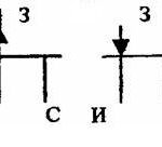
Switching schemes
To work in a single circuit, the transistor requires 2 outputs at the input and output. Almost all types of semiconductor devices have only 3 connection points. To get out of a difficult situation, one of the ends is assigned as a common one. This leads to 3 common connection schemes:
- for bipolar transistor;
- polar device;
- with an open drain (collector).
The bipolar module is connected with a common emitter for both voltage and current (MA) amplification. In other cases, it matches the pins of a digital chip when there is a large voltage between the outer circuit and the inner connection plan.This is how the common collector connection works, and only an increase in current (OK) is observed. If you need to increase the voltage, then the element is introduced with a common base (OB). The option works well in compound cascade circuits, but is rarely set in single-transistor projects.
Field semiconductor devices of MIS varieties and using a p-n junction are included in the circuit:
- with a common emitter (CI) - a connection similar to the OE of a bipolar type module
- with a single output (OS) - a plan of the OK type;
- with a joint shutter (OZ) - a similar description of the OB.
In open-drain plans, the transistor is switched on with a common emitter as part of the microcircuit. The collector output is not connected to other parts of the module, and the load goes to the external connector. The choice of voltage intensity and collector current strength is made after the installation of the project. Open-drain devices work in circuits with powerful output stages, bus drivers, TTL logic circuits.
What are transistors for?
The scope is delimited depending on the type of device - bipolar module or field. Why are transistors needed? If a low current is needed, for example, in digital plans, field views are used. Analog circuits achieve high gain linearity across a range of supply voltages and outputs.
Installation areas for bipolar transistors are amplifiers, their combinations, detectors, modulators, transistor logistics circuits, and logic-type inverters.
Places of application of transistors depend on their characteristics. They work in 2 modes:
- in an amplifying manner, changing the output pulse with small deviations of the control signal;
- in the key regulation, controlling the power supply of loads with a weak input current, the transistor is completely closed or open.
The type of semiconductor module does not change the conditions of its operation. The source is connected to the load, for example, a switch, an amplifier, a lighting device, it can be an electronic sensor or a powerful neighboring transistor. With the help of current, the operation of the load device begins, and the transistor is connected to the circuit between the installation and the source. The semiconductor module limits the strength of the energy supplied to the unit.
The resistance at the output of the transistor is transformed depending on the voltage on the control conductor. The current strength and voltage at the beginning and end point of the circuit change and increase or decrease and depend on the type of transistor and how it is connected. The control of a controlled power supply leads to an increase in current, a power pulse or an increase in voltage.
Transistors of both types are used in the following cases:
- In digital regulation. Experimental designs of digital amplifying circuits based on digital-to-analog converters (DAC) have been developed.
- in pulse generators. Depending on the type of assembly, the transistor operates in a key or linear order to reproduce square or arbitrary signals, respectively.
- In electronic hardware devices. To protect information and programs from theft, illegal hacking and use. The operation takes place in the key mode, the current strength is controlled in analog form and is regulated using the pulse width.Transistors are placed in the drives of electric motors, switching voltage stabilizers.
Monocrystalline semiconductors and open and close modules increase power, but function only as switches. In digital devices, field-type transistors are used as economical modules. Manufacturing technologies in the concept of integrated experiments provide for the production of transistors on a single silicon chip.
The miniaturization of crystals leads to faster computers, less power and less heat.
Similar articles: