The use of semiconductor devices (SS) is widespread in radio electronics. Due to this, the dimensions of various devices have decreased. The bipolar transistor has received wide application, due to some features its functionality is wider than that of a simple field-effect transistor. To understand why it is needed and under what conditions it is used, it is necessary to consider its principle of operation, connection methods and classification.
Content
Device and principle of operation
A transistor is an electronic semiconductor consisting of 3 electrodes, one of which is a control one. A bipolar type transistor differs from a polar one in the presence of 2 types of charge carriers (negative and positive).
Negative charges are electrons that are released from the outer shell of the crystal lattice. A positive type of charge, or holes, are formed in place of the released electron.
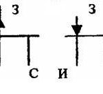
The device of a bipolar transistor (BT) is quite simple, despite its versatility. It consists of 3 layers of conductive type: emitter (E), base (B) and collector (C).
An emitter (from the Latin "to release") is a type of semiconductor junction whose main function is to inject charges into the base. The collector (from the Latin "collector") serves to receive the charges of the emitter. The base is the control electrode.
The emitter and collector layers are almost the same, but differ in the degree of addition of impurities to improve the characteristics of the PCB. The addition of impurities is called doping. For the collector layer (CL), doping is weakly expressed to increase the collector voltage (Uc). The emitter semiconductor layer is heavily doped in order to increase the reverse allowable breakdown U and improve the injection of carriers into the base layer (the current transfer coefficient increases - Kt). The base layer is lightly doped to provide more resistance (R).
The transition between the base and the emitter is smaller in area than the K-B. Due to the difference in areas, the improvement of Kt occurs. During the operation of the PCB, the K-B transition is switched on with a reverse bias to release the main fraction of the amount of heat Q, which is dissipated and provides better cooling of the crystal.
The speed of BT depends on the thickness of the base layer (BS). This dependence is a value that varies in inverse proportion. With less thickness - more speed. This dependence is related to the time of flight of charge carriers.However, at the same time, Uk decreases.
A strong current flows between the emitter and K, called the current K (Ik). A small current flows between E and B - current B (Ib), which is used for control. When Ib changes, Ik changes.
The transistor has two p-n junctions: E-B and K-B. When the mode is active, E-B is connected with a forward type bias, and CB is connected with a reverse bias. Since the E-B transition is in the open state, negative charges (electrons) flow into the B. After that, they partially recombine with holes. However, most of the electrons reach K-B due to the low legitimacy and thickness of B.
In BS, electrons are minor charge carriers, and the electromagnetic field helps them overcome the K-B transition. With an increase in Ib, the E-B opening will expand and more electrons will run between E and K. In this case, a significant amplification of the low-amplitude signal will occur, since Ik is greater than Ib.
In order to more easily understand the physical meaning of the operation of a bipolar type transistor, it is necessary to associate it with a good example. It must be assumed that the pump for pumping water is a power source, the water tap is a transistor, water is Ik, the degree of rotation of the tap handle is Ib. To increase the pressure, you need to slightly turn the tap - to perform a control action. Based on the example, we can conclude a simple principle of operation of the software.
However, with a significant increase in U, impact ionization can occur at the K-B transition, which results in avalanche charge multiplication.When combined with the tunnel effect, this process gives an electrical, and with an increase in time, a thermal breakdown, which disables the PP. Sometimes thermal breakdown occurs without electrical breakdown as a result of a significant increase in current through the collector output.
In addition, when U changes to K-B and E-B, the thickness of these layers changes, if B is thin, then a closure effect occurs (it is also called a puncture B), in which the transitions K-B and E-B are connected. As a result of this phenomenon, the PP ceases to perform its functions.
Operating modes
The bipolar type transistor can operate in 4 modes:
- Active.
- Cutoffs (RO).
- Saturation (PH).
- Barrier (RB).
The active mode of BT is normal (NAR) and inverse (IAR).
Normal active mode
In this mode, U flows at the E-B junction, which is direct and is called the E-B voltage (Ue-b). The mode is considered optimal and is used in most schemes. Transition E injects charges into the base region, which move towards the collector. The latter accelerates the charges, creating a boost effect.
Inverse active mode
In this mode, the K-B transition is open. The BT works in the opposite direction, i.e., hole charge carriers are injected from K, passing through the B. They are collected by the E transition. The amplification properties of the PP are weak, and BTs are rarely used in this mode.
Saturation mode
At PH, both transitions are open. When E-B and K-B are connected to external sources in the forward direction, the BT will work in the launch vehicle. The diffusion electromagnetic field of the E and K junctions is weakened by the electric field, which is created by external sources.As a result of this, there will be a decrease in the barrier ability and a limitation of the diffuse ability of the main charge carriers. The injection of holes from E and K to B will begin. This mode is used mainly in analog technology, but in some cases there may be exceptions.
Cutoff mode
In this mode, the BT closes completely and is not able to conduct current. However, in the BT there are insignificant flows of minor charge carriers, which create thermal currents with small values. This mode is used in various types of protection against overloads and short circuits.
barrier regime
The BT base is connected through a resistor to K. A resistor is included in the K or E circuit, which sets the current value (I) through the BT. BR is often used in circuits, because it allows the BT to operate at any frequency and over a larger temperature range.
Switching schemes
For the correct use and connection of BTs, you need to know their classification and type. Classification of bipolar transistors:
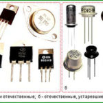
- Production material: germanium, silicon and arsenidogallium.
- Manufacturing features.
- Dissipated power: low-power (up to 0.25 W), medium (0.25-1.6 W), powerful (above 1.6 W).
- Limiting frequency: low-frequency (up to 2.7 MHz), mid-frequency (2.7-32 MHz), high-frequency (32-310 MHz), microwave (more than 310 MHz).
- Functional purpose.
The functional purpose of BT is divided into the following types:
- Amplifying low-frequency ones with normalized and non-normalized noise figure (NiNNKSh).
- Amplifying high-frequency with NiNNKSh.
- Amplifying microwave with NiNNKSh.
- Amplifying powerful high-voltage.
- Generator with high and ultrahigh frequencies.
- Low-power and high-power high-voltage switching devices.
- Powerful pulsed for high U-values.
In addition, there are such types of bipolar transistors:
- P-n-p.
- N-p-n.
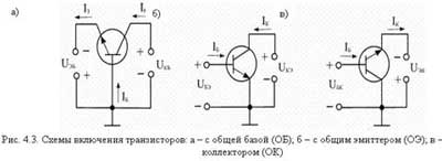
There are 3 circuits for switching on a bipolar transistor, each of which has its own advantages and disadvantages:
- General B.
- General E.
- General K.
Switching on with a common base (OB)
The circuit is applied at high frequencies, allowing optimal use of the frequency response. When connecting one BT according to the scheme with OE, and then with OB, its frequency of operation will increase. This connection scheme is used in antenna-type amplifiers. The noise level at high frequencies is reduced.
Advantages:
- Optimal temperatures and wide frequency range (f).
- High value Uk.
Flaws:
- Low I gain.
- Low input R.
Common-Emitter Switching (CE)
When connected according to this scheme, amplification occurs in U and I. The circuit can be powered from a single source. Often used in power amplifiers (P).
Advantages:
- High gains for I, U, P.
- One power supply.
- The output variable U is inverted relative to the input.
It has significant disadvantages: the lowest temperature stability and frequency characteristics are worse than when connected with OB.
Switching on with a common collector (OK)
The input U is fully transferred back to the input, and Ki is similar when connected with an OE, but it is low in U.
This type of switching is used to match cascades made on transistors, or with an input signal source that has a high output R (condenser-type microphone or pickup). The advantages include the following: a large value of the input and a small output R.The disadvantage is the low U gain.
Main characteristics of bipolar transistors
The main characteristics of BT:
- I gain.
- Input and output R.
- Reverse Ik-e.
- Turn-on time.
- Transmission frequency Ib.
- Reverse Ik.
- Maximum I value.
Applications
The use of bipolar transistors is widespread in all areas of human activity. The main application of the device was received in devices for amplification, generation of electrical signals, and also serve as a switched element. They are used in various power amplifiers, in ordinary and switching power supplies with the ability to adjust the values of U and I, in computer technology.
In addition, they are often used to build various consumer protection against overloads, U surges, and short circuits. They are widely used in the mining and metallurgical industries.
Similar articles: